State Machine
Charts
State Machine Design with SM Charts
Another name for a sequential circuit is an algorithmic state
machine or simply a state machine, named for the sequential
circuit that is used to control a digital system that carries out a
step-by-step procedure or algorithm.
As an alternative to using state graphs, a special type of
flowchart, called a state machine flowchart or SM chart, may be used to
describe the behavior of a state machine
State Machine Charts
SM charts are also called ASM (algorithmic state machine)
charts.
Advantages:
1.
It is often easier to understand the
operation of a digital system by inspection of the SM chart instead of the
equivalent state graph.
2.
A given SM chart can be converted into
several equivalent forms, and each form leads directly to a hardware
realization.
An SM chart differs from an ordinary flowchart in that certain
specific rules must be followed in constructing the SM chart. When these rules
are followed, the SM chart is equivalent to a state graph, and it leads
directly to a hardware realization.
Fig.1 shows the three principal components of an SM chart.
The state of the system is represented by a state box. The state box contains a state name, and it may contain an output list. A state
code may be placed outside the box at the top.
A decision
box is represented by a diamond-shaped symbol
with true and false branches. The condition
placed in the box is a Boolean expression
that is evaluated to determine which branch to take.
The conditional
output box, which has curved ends, contains a conditional output list.The conditional outputs depend on both
the state of the system and the inputs.
An SM chart is constructed from SM blocks.
Each SM block, contains exactly one state box together with the decision boxes
and conditional output boxes associated with that state.
An SM block has exactly one entrance path and
one or more exit paths. Each SM block describes the machine
operation during the time that the machine is in one state.When a digital
system enters the state associated with a given SM block, the outputs on the
output list in the state box become true.
The conditions in the decision boxes are evaluated to determine
which path (or paths) is (are) followed through the SM block.When a conditional
output box is encountered along such a path, the corresponding conditional
outputs become true. A path through an SM block from entrance to exit is
referred to as a link path.
From Fig.2, when state S1
is entered, outputs Z1 and Z2
become 1. If inputs X1 and X2
are both equal to 0, Z3 and Z4
are also 1, and at the end of the state time, the machine goes to the next
state via exit path 1. On the other hand, if X1 =1 and X3 = 0,
the output Z5 is 1, and an exit to the next state will occur via exit path
3.
A given SM block can generally be drawn in several different
forms as shown in fig.3. In both Fig.3(a) and (b), the output Z2=1 if X1 = 0;
the next state is S2 if X2
= 0 and S3 if X2
= 1.
Consider a Combinational circuit where
only one state occurs and the state doesn’t change, i.e.,
Z1= A+A’BC = A + BC
Rules to be followed while constructing an SM block:
1.
For every valid combination of input
variables, there must be exactly one exit path defined. This is necessary
because each allowable input combination must lead to a single next state.
2.
No internal feedback within an SM block is
allowed.
An SM block can have several parallel paths which lead to the
same exit path as shown in fig.6 (a), and more than one of these paths can be
active at the same time. Eg., if X1 = X2 = 1
and X3 = 0, the link paths marked with dashed lines
are active, and the outputs Z1, Z2,
and Z3 will be l. Although this would not be a valid flowchart for a
program for a serial computer, it presents no problems for a state machine
implementation. The state machine can have a multiple-output circuit that generates
Z1, Z2, and Z3
at the same time.
In the serial SM block as shown in fig.6 (b) only one active
link path between entrance and exit is possible. For any combination of input
values the outputs will be the same as in the equivalent parallel form. The
link path forX1=X2=1
and X3=0 is shown with a dashed line, and the outputs encountered on
this path are Z1, Z2,
and Z3. Regardless of whether the SM block is drawn in serial or
parallel form, all of the tests take place within one clock time.
Conversion of a state graph for a
sequential machine into an equivalent SM chart:
The state graph of Fig.7(a) has both Moore and Mealy outputs.
The equivalent SM chart has three blocks - one for each state. The Moore
outputs (Za, Zb and Zc)
are placed in the state boxes because they do not depend on the input. The
Mealy outputs (Z1 and Z2)
appear in conditional output boxes as they depend on both the state and input.
Each SM block has only one decision box as only one input
variable must be tested. For both the state graph and SM chart, Zc is always 1 in state S2.
If X=0 in state S2, Z1 =1 and the next state is S0.
If X = 1,
Z2 = 1 and the next state is S2.
Fig.8 shows a timing chart for the SM chart with an input
sequence X = 1,
1, 1, 0, 0, 0. All state changes occur immediately after the rising edge of the
clock.
Since the Moore outputs (Za,Zb and Zc) depend on the state, they can only
change immediately following a state change.
The Mealy outputs (Z1 and Z2) can change immediately
after a state change or an input change. In any case, all outputs will have
their correct value during the active edge of the clock.
Fig.7: Conversion of a state Graph to an SM Chart
Fig.8: Timing Chart
Derivation of SM Charts
Method
used to derive an SM chart for a sequential control circuit:
1. Draw
a block diagram of the system we are controlling.
2. Define
the required input and output signals to and from the control circuit.
3. Construct
an SM chart that tests the input signals and generates the proper sequence of
output signals.
Examples of SM
charts:
1. An SM Chart for the control of the binary
multiplier
SM Chart for
Binary Multiplier
The
add-shift control generates the required sequence of add and shift signals. The
Counter counts the number of shifts and outputs K=1 just before the last shift
occurs.
In
State S0, when the start signal St=1, the registers are loaded. In S1,
the multiplier bit M is tested, if M=1, an add signal is generated and the next
state is S2. If M=0, a shift signal is generated and K is tested. If
K=1, this will be the last shift and the next state is S3.
In S2, a shift signal is generated, as a shift must
always follow an add. If K=1, the network goes to S3 at the time of
the last shift, else the next state is S1. In S3, the
done signal is turned on.
Verilog Code for the Binary Multiplier:
module(clk,st,k,m,load,sh.ad,done);
input
clk,st,k,m;
output
load,sh,ad,done;
reg/wire
[3:0]state, nextstate;
always@(st,k,m,state)
begin
load<=1’b0;
sh<=1’b0;
Ad<=1’b0;
Case(state)
1’d0:
if(st==1)
begin
load<=1’b1;
nextstate<=1’d1;
end
else
nextstate<=1’d0;
1’d1:
if(m==1)
begin
ad<=1’b1;
nextstate<=1’d2;
end
else
begin
sh<=1’b1;
if(k==1)
nextstate<=1’d3;
else
nextstate<=1’d1;
end
1’d2:
sh<=1’b1;
if(k==1)
nextstate<=1’d3;
else
nextstate<=1’d1;
1’d3:
done<=1’b1;
Nextstate<=1’b0;
endcase
end
always@(clk)
begin
if(clk)
state<=nextstate;
end
endmodule
2. An SM chart for control of the parallel
binary divider
The
binary division requires a series of subtract and shift operations. S0 is the starting state. In S0, the start signal (St) is tested, and if St = 1,
the Load signal
is turned on and the next state is S1. In S1,
the compare signal (C)
is tested. If C =
1, the quotient would be larger than 4
bits, so an overflow signal (V = 1) is generated and the state changes back
to S0.
If
C =
0, Sh
becomes 1, so at the next clock the
dividend is shifted to the left and the state changes to S2. C
is tested again in state S2. If C
= 1,
subtraction is possible, so Su becomes
1 and no state change occurs. If C = 0, Sh
= 1,
and the dividend is shifted as the state changes to S3.The action in states S3 and S4
is identical to that in state S2. In state S5
the next state is always S0,
and C =
1 causes subtraction to occur.
3.
Design
of an electronic dice game
Two counters are used to simulate the roll of the dice. Each
counter counts in the sequence 1, 2, 3, 4, 5,6,1,2, . . . .Thus, after the
“roll” of the dice, the sum of the values in the two counters will be in the
range 2 through 12.
The
rules of the game are as follows:
1. After
the first roll of the dice, the player wins if the sum is 7 or 11. He loses if
the sum is 2, 3, or 12. Otherwise, the sum which he obtained on the first roll
is referred to as his point, and he must roll the dice again.
2. On
the second or subsequent roll of the dice, he wins if the sum equals his point,
and he loses if the sum is 7. Otherwise, he must roll again until he finally
wins or loses.
The
inputs to the dice game come from two push buttons, Rb
(roll button) and
Reset. Reset is used to initiate a new game. When the roll
button is pushed, the dice counters count at a high speed, so the values cannot
be read on the display.
When the roll button is released, the values in the two
counters are displayed and the game can proceed. Because the button is released
at a random time, this simulates a random roll of the dice. If the Win light or
Lose light is not on, the player must push the roll button again.
We will assume that the push buttons are properly debounced and
that the changes in Rb are
properly synchronized with the clock. Methods for debouncing and
synchronization are as discussed previously.
Fig.10 shows a flowchart for the dice game. After rolling the
dice, the sum is tested. If it is 7 or 11, the player wins; if it is 2, 3, or
12, he loses. Otherwise, the sum is saved in the point register, and the player
rolls again. If the new sum equals the point, he wins; if it is 7, he loses.
Otherwise, he rolls again. After winning or losing, he must push Reset to begin
a new game.
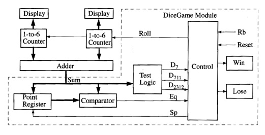
The components for the dice game shown in the block diagram
(Fig.9) include an adder which adds the two counter outputs, a register to
store the point, test logic to determine conditions for win or lose, and a
control circuit.
The
input signals to the control circuit are defined as:
D7 = 1
if the sum of the dice is 7
D711
= 1
if the sum of the dice is 7 or 11
D2312 = 1
if the sum of the dice is 2, 3, or 12
Eq
= 1
if the sum of the dice equals the number stored in the point register
Rb=_ 1 when the roll button is pressed
Reset
= 1
when the reset button is pressed
The
outputs from the control circuit are defined as follows:
Roll
= 1
enables the dice counters
Sp
= 1
causes the sum to be stored in the point register
Win
= 1
turns on the win light
Lose
= 1
turns on the lose light
Fig.11:
SM Chart for Dice Game
The resultant flowchart for the dice game to an SM chart for
the control circuit using the defined control signals is as shown in Fig.11.
The control circuit waits in state S0 until the roll button is pressed (Rb = 1).Then, it goes to state S1, and the roll counters are enabled as long as Rb = 1.
As
soon as the roll button is released (Rb
= 0),D711
is tested. If the sum is 7 or 11, the circuit goes to state S2 and turns on the Win light; otherwise,D2312
is tested. If the sum is 2, 3, or 12, it goes to state S3 and turns on the Lose light; otherwise,
the signal Sp becomes 1, and the sum is stored in the point register. It then
enters S4 and waits for the player to “roll the dice” again.
In
S5,
after the roll button is released, if Eq
= l,
the sum equals the point and state S2 is entered to indicate a win. If D7 = 1,
the sum is 7 and S3
is entered to indicate a loss. Otherwise, the control returns to S4 so that the player can roll again. When
in S2
or S3,
the game is reset to S0
when the Reset button is pressed. Instead of using an SM chart, we could
construct an equivalent state graph from the flowchart.
Verilog module for the Dice Game SM Chart
(Behavioral):-
module(rb,reset,clk,sum,roll,win,lose);
input
rb,reset,clk;
input
[12:2]sum;
output
roll,win,lose;
wire/reg
[5:0]state,nextstate;
wire/reg
[12:2]point;
wire/reg
sp;
always@(rb,reset,sum,state)
begin
sp<=1’b0;
roll<=1’b0; win<=1’b0; lose<=1’b0;
case(state)
1’d0:
if(rb==1)
nextstate<=1’d1;
1’d1:
if(rb==1) roll<=1’b1;
else if((sum==7)|(sum=11))
nextstate<=1’d2;
else if((sum==2)|(sum=3)|(sum=12))
nextstate<=1’d3;
else
begin
sp<=1’b1;
nextstate<=1’d4;
end
1’d2:
win<=1’b1;
if(reset==1)
nextstate<=1’d0;
1’d3:
lose<=1’b1;
if(reset==1)
nextstate<=1’d0;
1’d4:
if(rb==1)
nextstate<=1’d5;
1’d5:
if(rb==1)
roll<=1’b1;
else if(sum=point)
nextstate<=1’d2;
else if(sum=7)
nextstate<=1’d3;
else
nextstate<=1’d4;
endcase
end
always@(clk)
begin
if(posedge
(clk))
state<=nextstate;
if(sp==1)
point<=sum;
end
endmodule
Fig.12.1:
Dice Game with Test Bench
Fig.12.2:
SM Chart for Dice Game Test
module
gametest(rb,reset,sum,clk,roll,win,lose);
output
rb,reset;
output[12:2]
sum;
inout
clk;
input
roll,win,lose;
wire[3:0]
tstate,tnext;
wire
trig1;
wire
i;
mem
[11:0]arr;
parameter
sumarray={7,11,2,4,7,5,6,7,6,8,9,6};
always
#20 clk=~clk;
always@(roll,win,lose,tstate)
begin
case(tstate)
1’d0:
rb=1’b1;
Reset=1’b0;
if(i>=12)
begin
tnext=1’d3;
else
if(roll= =1)
begin
sum=sumarray[i];
i=i+1’d1;
tnext=1’d1;
end
end
1’d1: rb=1’b0;
Tnext=1’d2;
1’d2: tnext=1’d0;
Trig1=~trig1;
if((win|lose) = =1) reset=1’b1;
1’d3:
null;
endcase;
end
always@(posedge
clk)
begin
if(clk=
=1) tsate=tnext;
end
endmodule
module
test_tester();
reg/wire
rb1,reset1,clk1,roll1,win1,lose1;
reg/wire
[12:2] sum1;
dicegame
d1(rb1,reset1,clk1,sum1,roll1,win1,lose1);
gametest
g1(rb1,reset1,sum1,clk1, roll1,win1,lose1);
endmodule
module
test_tester_tb();
reg ;
wire ;
test_tester
t1();
initial
begin
trig1=1’b0;
sum1=1’d2; point=1’d2;
#580
trig1=1’b1;
#900
trig1=1’b0;
#1060
trig1=1’b1;
#1380
trig1=1’b0;
#1540
trig1=1’b1;
#1700
trig1=1’b0;
end
initial
$monitor($time, “ trig1=5b, sum1=%d, win1=%b,lose1=%b,point=%d”,
trig1,sum1,win1,lose1,point);
initial
#2000 $finish;
endmodule
Simulation and Command File for Dice Game
Tester
Fig.13: State Graph for Dice Game Controller
The state graph is
as shown in Fig.13 for the dice game controller. The state graph has the same
states, inputs, and outputs as the SM chart. The arcs have been labeled
consistently with the rules for proper alphanumeric state graphs. Thus, the
arcs leaving state S1
are labeled Rb,
Rb’D711, Rb’D’711D2312,
and Rb’D’711D’2312.With
these labels, only one next state is defined for each combination of input values.
Note that the structure of the SM chart automatically defines only one next
state for each combination of input values.
Realization of SM Charts
The methods used are similar to the methods used to
realize state graphs. As with any sequential circuit, the realization will
consist of a combinational subcircuit together with flip-flops for storing the
state of the circuit.
In some cases, it may be possible to identify equivalent
states in an SM chart and eliminate redundant states using the same method as
was used for reducing state tables. However, an SM chart is usually
incompletely specified in the sense that all inputs are not tested in every
state, which makes the reduction procedure more difficult. Even if the number
of states in an SM chart can be reduced, it is not always desirable to do so
because combining states may make the SM chart more difficult to interpret.
Before deriving next-state and output equations from an SM
chart, a state
assignment must be made.The best way of making the assignment
depends on how the SM chart is realized. If gates and flip-flops (or the
equivalent PLD realization) are used.
Fig.1 State Machine Chart
Eg., consider Fig.1, The state assignment AB _ 00
for S0,AB _ 01 for S1, and AB _ 11 for S2.
After a state assignment has been made, output and next-state equations can be
read directly from the SM chart. Because the Moore output Za is 1 only
in state 00, Za _ AB. Similarly, Zb _ AB and Zc _ AB.
The conditional output Z1 _ ABX because the only link path
through Z1 starts with AB _ 11 and takes the X _ 0 branch.
Similarly, Z2 _ ABX.
There are three link paths (labeled link 1, link 2, and
link 3), which terminate in a state that has B _ 1. Link 1 starts with a
present state AB _ 00, takes the X _ 1 branch, and terminates on
a state in which B _ 1.Therefore, the next state of B (B_)
equals 1 when ABX _ 1. Link 2 starts in state 01, takes the X _ 1
branch, and ends in state 11, so B_ has a term ABX. Similarly, B_
has a term ABX from link 3. The next-state equation for B thus
has three terms corresponding to the three link paths: B+ = A’B’X +
A’ BX + ABX = link1 + link2 + link3
Similarly, two link paths terminate in a state with A = 1,
so A+ =A’BX + ABX
These output and next-state equations can be simplified
with a Karnaugh map, using the unused state assignment (AB =10) as a don’t-care
condition.
The next-state equation for a flip-flop Q can be derived
from the SM chart as follows:
1. Identify
all of the states in which Q = 1.
2. For
each of these states, find all of the link paths that lead into the state.
3. For
each of these link paths, find a term that is 1 when the link path is followed.
i.e., for a link path from Si to Sj, the term will be 1
if the machine is in state Si and the conditions for exiting to Sj
are satisfied.
4. The
expression for Q+(the next state of Q) is formed by ORing together
the terms found in step 3.
Fig.2: SM Chart for control of a
binary multiplier
Next, to implement the multiplier control SM chart of
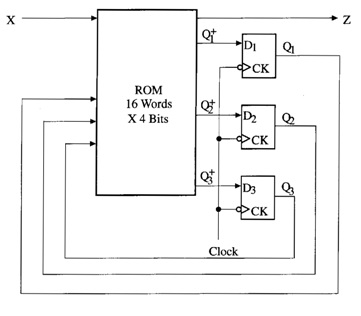
Fig.2 using a PLA or a ROM and two D flip-flops connected, as shown in Fig.3.
Fig.3: Realization of a Mealy
Sequential Network with a ROM
The PLA has five inputs and six outputs. We will use a straight
binary state assignment (S0=00, S1= 01, etc.). Each row
in the PLA table (Table.1) corresponds to one of the link paths in the SM
chart. Because S0 has two exit paths, the table has two rows for
present state S0. Because only St is tested in S0,
M and K are don’t-cares as indicated by dashes. The first row corresponds to
the St = 0 exit path, so the next state is 00 and all outputs are 0.In the
second row, St =1, so the next state is 01 and the other PLA outputs are 1000.
Because St is not tested in states S1, S2, and S3,
St is a don’t-care in the corresponding rows. The outputs for each row can be
filled in by tracing the corresponding link paths on the SM chart. For example,
the link path from S1 to S2 passes through conditional output Ad when M=1, so
Ad=1 in this row. Because S2 has a Moore output Sh, Sh =1 in both of the rows
for which AB=10.
Table.1:
PLA table for Multiplier Control
If a ROM is used instead of a PLA, the PLA table must be
expanded to 25=32 rows since there are five inputs. To expand the
table, the dashes in each row must be replaced with all possible combinations
of 0s and 1s. if a row has n dashes, it must be replaced with 2n
rows.
The added entries are printed in boldface. By inspection
of the PLA table, the logic equations for the multiplier control are
A+=A’BM’K + A’BM + AB’K = A’B (M+K) + AB’K
B+=A’B’St + A’BM’(K’+K) + AB’(K’+K) = A’B’St +
A’BM’ + AB’
Load = A’B’St
Sh = A’BM’(K’+K) + AB’(K’+K) = A’BM’ + AB’
Ad = A’BM’
Done = AB
Implementation of the Dice Game
The SM chart for the dice game controller can be
implemented using a PLA and three D flip-flops, as shown in Fig.4.
Fig.4: SM Chart for Dice Game
Fig.5: PLA Realization of Dice Game
The PLA has nine inputs and seven outputs, which are
listed at the top of Table-2. It has one row for each link path on the SM
Chart. In state ABC= 000, the next state is A+B+C+=000
or 001, depending on the value of Rb. Since state 001 has four exit paths, the
PLA table has four corresponding rows. When Rb is 1, Roll is 1 and there is no
state change. When Rb=0 and D711 is 1, the next state is 010.When
Rb=0 and D2312=l, the next state is 011.For the link path from state
001 to 100, Rb, D711, and D2312 are all 0, and Sp is a
conditional output. This path corresponds to row 4 of the PLA table, which has
Sp=1 and A+B+C+=100.
Table-2: PLA Table for Dice Game
In state 010, the Win signal is always on, and the next
state is 010 or 000, depending on the value of Reset. Similarly Lose is always
on in state 011. In state 101, A+B+C+=010 if Eq=1; otherwise, A+B+C+=011 or
100, depending on the value of D7. Since States 110 and 111 are not
used, the next states and outputs are don’t cares when ABC=110 or 111.
The Dice game controller can also be realized using a PAL.
The required PAL equations can be derived from table-2 using the method of
map-entered variables or using a CAD program such as LogicAid.
Fig.6: Maps derived from Table-2.
Since A,B,C, and Rb have assigned values in most of the
rows of the table, these four variables are used on the map edges, and the
remaining variables are entered within the map. E1,E2,E3,E4
and E5 represent the expressions. From the A+ column in
the PLA table, A+ is 1 in row 4, so we should enter D’711D’2312
in the ABCRb=0010 square of the map. To save space, we define E1=D’711D’2312
and place E1 in the square. Since A+ is 1 in rows 11,12,
and 16, 1s are placed on the map squares ABCRb=1000, 1001, 1011. From row 13,
we place E2=D’7Eq’ in the 1010 square. In rows 7 and 8,
Win is always 1 when ABC=010, so 1s are plotted in the corresponding squares of
the Win map.
The resulting PAL equations (can also be derived by
tracing link paths on the SM chart and simplifying them using don’t care next
states) are
A+ = A’B’C Rb’D’711D’2312
+ AC’ + A Rb + AD’7Eq’
B+ = A’B’C Rb’(D711+D2312)
+ BReset’ + AC Rb’(Eq+D7)
C+ = B’Rb + A’B’C D’711D2312
+ BC Reset’ + AC D7Eq’
Win = BC’
Lose = BC
Roll = B’CRb
Sp=A’B’C Rb’D’711D’2312
These equations can be implemented using a 16R4 PAL with
no external components. The entire dice game including the control network, can
be implemented using a programmable gate array.
Dataflow model for the dice game controller based on the
block diagram shown in fig.7.
Fig.7: Block Diagram for Dice Game
Dataflow model of Dice game:
module dicegame_diceeq(sp,eq,d7,d711,d2312,da,db,dc,a,b,c,point);
input sp,eq,d7,d711,d2312,da,db,dc,a,b,c;
input [12:2]point;
reg sp,eq,d7,d711,d2312,da,db,dc,a,b,c;
reg [12:2]point;
always@(clk)
begin
if(posedge clk)
begin
a=da;
b=db;
c=dc;
if(sp= =1)
point=sum;
end
end
win=b&(~c);
lose=b&c;
roll=(~b)&(c&rb);
sp=(((~a)&(~b))&(c&(~rb)))&((~d711)&(~d2312));
if(sum=1’d7)
begin
d7=1’b1;
else
d7=1’d0;
end
if((sum= =11)|(sum= =7))
begin
d711=1’b1;
else
d711=1’b0;
end
if((sum= =2)|((sum= =3)|(sum=12)))
d2312=1’b1;
else
d2312=1’b0;
end
if(point= = sum)
begin
eq=1’b1;
else
eq=1’b0;
end
da=(((~a)&(~b)&c&(~rb)&(~d711)&(~d2312)|a&(~c)|a&rb|(a&(~d7)&(~eq));
db=((~a)&((~b)&c))&(((~rb)&(d711|d2312))|(b&(~reset)))|(((a&c)&(~rb))&(eq|d7));
dc=(~b)&rb|(~a)&(~b)&c&(~d711&d2312)|b&c&(~reset)|(a&(c&d7)&(~eq));
endmodule
The always statement updates the
flip-flop states and the point register when the rising edge of clock occurs.
Generation of the control signals and D flip-flop input equations is done using
concurrent statements. In particular D7,D711, D2312
and Eq are implemented using conditional signal assignments.
Alternatively, all the signals and D
input equations can be implemented in behavior model using always statement
with a sensitivity list containing A, B, C, Sum, Point, Rb, D7, D711,
D2312, Eq, and Reset. Whose architecture is shown in fig.7, same as
that of dataflow model and the test bench is shown in fig.8. The results will
be identical.
Fig.8: SM
Chart for Dice Game Test
module
gametest(rb,reset,sum,clk,roll,win,lose);
output rb,reset;
output[12:2] sum;
inout clk;
input roll,win,lose;
wire[3:0] tstate,tnext;
wire trig1;
wire i;
mem [11:0]arr;
parameter
sumarray={7,11,2,4,7,5,6,7,6,8,9,6};
always #20 clk=~clk;
always@(roll,win,lose,tstate)
begin
case(tstate)
1’d0: rb=1’b1;
Reset=1’b0;
if(i>=12)
begin
tnext=1’d3;
else
if(roll= =1)
begin
sum=sumarray[i];
i=i+1’d1;
tnext=1’d1;
end
end
1’d1:
rb=1’b0;
Tnext=1’d2;
1’d2:
tnext=1’d0;
Trig1=~trig1;
if((win|lose) = =1) reset=1’b1;
1’d3: null;
endcase;
end
always@(posedge clk)
begin
if(clk= =1) tsate=tnext;
end
endmodule
module test_tester();
reg/wire
rb1,reset1,clk1,roll1,win1,lose1;
reg/wire [12:2] sum1;
dicegame
d1(rb1,reset1,clk1,sum1,roll1,win1,lose1);
gametest g1(rb1,reset1,sum1,clk1,
roll1,win1,lose1);
endmodule
module test_tester_tb();
reg ;
wire ;
test_tester t1();
initial
begin
trig1=1’b0; sum1=1’d2; point=1’d2;
#580 trig1=1’b1;
#900 trig1=1’b0;
#1060 trig1=1’b1;
#1380 trig1=1’b0;
#1540 trig1=1’b1;
#1700 trig1=1’b0;
end
initial $monitor($time, “ trig1=5b,
sum1=%d, win1=%b,lose1=%b,point=%d”, trig1,sum1,win1,lose1,point);
initial #2000 $finish;
endmodule
To complete the Veriolg
implementation of the Dice Game, we add two modulo-six counters as shown in modules
counter and game. The counters are initialized to 1, so the sum of the two dice
will always be in the range 2 through 12. When Cntl is in state 6, the next
clock sets it to state 1, and Cnt2 is incremented (or Cnt2 is set to 1 if it is
in state 6).
module counter(clk,roll,sum);
input clk,roll;
output[12:2] sum;
wire [6:1]cnt1,cnt2;
parameter cnt1=1’d1;
parameter cnt2=1’d1;
always@(posedge clk)
begin
if (clk= =1)
begin
if(roll= =1)
begin
if(cntl1= =6)
begin
cnt1=1’d1;
else
cnt1=cnt1+1’d1;
end
if((cnt1= =6) & (cnt2= =6))
begin
cnt2=1’d1;
else
cnt2=cnt2+1’d1;
end
end
end
end
sum=cnt1+cnt2;
endmodule
module game(rb,reset,clk,win,lose);
input rb,reset,clk;
output win, lose;
wire roll1;
wire [12:2]sum1;
dicegame
d1(rb,reset,clk,sum1,roll1,win,lose);
counter c1(clk,roll1,sum1);
endmodule
If a ROM is used instead of PLA, the PLA table must be
expanded to 29=512 rows. To expand the table, the dashes in each row
must be replaced with all possible combinations of 0’s and 1’s. eg., row5 could
be replaced with the following 8 rows.
LINKED STATE MACHINES
When a sequential machine becomes
large and complex, then the machine can be divided into several smaller
machines which are easier to design and implement and are linked together. Also
one of the submachines may be called in several different places by the main machine.
Fig.1:
SM Charts for serially linked state machines
From fig.1, the main machine (machine
A) executes a sequence of some states until it is ready to call the submachine
(machine B). when state SA is reached, the output signal ZA activates machine
B. machine B then leaves its idle state and executes a sequence of other
states. When it finishes, it outputs ZB before returning to the idle state.
When machine A receives ZB, it continues to execute other states. Assume that
the two machines have a common clock.
Consider fig.2, Rb is used to control
the roll of the dice in states S0 and S1 and in an identical way in states S4
and S5. As this function is repeated in two places, it is logical to use a
separate roll control (fig.3) which allows the main dice control to be reduced
from six states to four states. The main control generates an En_roll (enable
roll) signal in T0 and then waits for a Dn_roll (done rolling) signal before
continuing. Similar action occurs in T1. The roll control machine waits in
state S0 untill it gets an En_roll signal from the main dice game control.
Then, when the roll button is pressed (Rb=1), the machine goes to S1 and
generates a Roll signal. It remains in S1 until Rb=0, in which case the Dn_roll
signal is generated and the machine goes back to state S0.
Fig.2:
SM Chart for Dice Game
Fig.3:
Linked SM Charts for Dice Game